Nvidia's New AI Chip Design at GTC 2026: What SRAM Means for HBM Demand
Nvidia reveals a new SRAM-based AI inference chip at GTC 2026 in San Jose — a move that could reshape GPU memory markets and signals a decisive shift from training to the inference and agentic AI era.
Every year, the AI world watches Nvidia's GTC conference the way the tech world once watched Apple's product launches. And at GTC 2026, held March 16-19 in San Jose, California, Nvidia delivered something that genuinely changes the conversation — not just about AI hardware, but about the trillion-dollar memory market that has grown up around it.
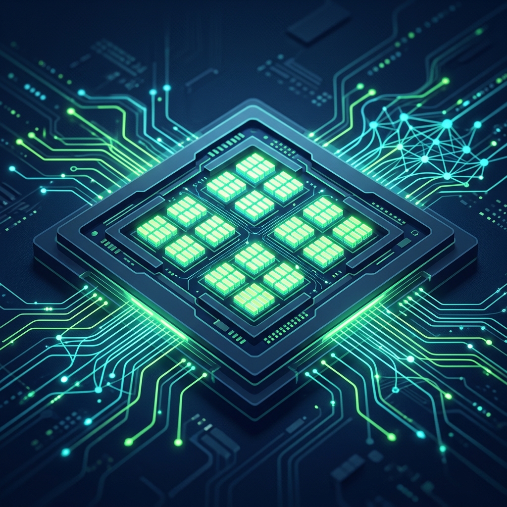
The company is preparing to unveil a new dedicated AI inference chip built around on-chip Static Random Access Memory (SRAM) rather than the High-Bandwidth Memory (HBM) that has defined AI chip architecture for the past several years. The announcement ripples outward in multiple directions simultaneously: it signals a fundamental architectural pivot, raises new questions about HBM manufacturers' futures, and — most importantly — reflects Jensen Huang's clear thesis that the AI industry is entering a new era defined by inference, not training.
The Training Era Is Over. The Inference Era Has Begun.
In his GTC 2026 keynote, Jensen Huang was unambiguous about where he sees AI heading. The period of massive investment in training enormous foundational models — GPT-4, Gemini Ultra, Claude 3 — is maturing. The new frontier, according to Huang, is inference and agentic AI: the phase where AI systems run in real time, make decisions autonomously, and execute complex multi-step tasks without human intervention.
This isn't semantic — it's architectural. Training workloads are characterized by enormous batch sizes, long computation sequences, and the need for massive memory bandwidth to feed parameters across GPUs. Inference is fundamentally different. It requires:
- Low latency — responses need to be generated in milliseconds, not minutes
- High throughput — serving millions of simultaneous user requests
- Memory efficiency — minimizing data movement between processor and memory
- Cost efficiency — inference happens billions of times daily at scale; cost per query is everything
Nvidia's single-GPU-architecture-for-everything approach (Hopper → Blackwell → Vera Rubin) has been extraordinarily effective for training. But for inference at massive scale, there is an emerging argument that a different architecture altogether may be optimal. That's the opening Nvidia is now moving to fill.
What Is SRAM and Why Does It Matter Over HBM?
To understand why Nvidia's new chip design is significant, you need to understand what separates SRAM from HBM (High-Bandwidth Memory).
HBM (High-Bandwidth Memory) is the type of stacked DRAM memory used in Nvidia's H100, H200, and upcoming Vera Rubin GPUs. It offers massive bandwidth — the H100 can move data at up to 3.35 terabytes per second — which makes it ideal for training workloads that need to stream enormous volumes of model parameters through the processor continuously. The tradeoff: HBM is expensive, constrained in supply, complex to manufacture, and physically located off-chip (requiring data to travel between the memory stack and the processor die).
SRAM (Static Random Access Memory) is a fundamentally different type of memory. It is:
- On-chip — embedded directly into the processor die, eliminating the latency of traveling off-chip
- Extremely fast — SRAM access times are measured in nanoseconds, versus tens of nanoseconds for HBM
- Lower power — SRAM doesn't need to be constantly refreshed like DRAM
- More expensive per bit — SRAM takes up significantly more silicon area than HBM equivalents
- Capacity-limited — you simply can't fit terabytes of SRAM on a chip the way you can stack HBM
For inference specifically, the SRAM trade-off is often favorable. Inference serves one request at a time with a specific model — the amount of data that needs to move is smaller and more predictable than training. The premium on latency (how fast you get a response) over bandwidth (how much data you can move in bulk) plays to SRAM's strengths.
This is exactly the philosophy behind the Groq LPU — Groq's Language Processing Unit, which Nvidia acquired and which appears to be the technical foundation for the new inference chip. Groq built its entire architecture around vast amounts of on-chip SRAM, achieving remarkable inference speeds by eliminating off-chip memory bottlenecks entirely.
The HBM Question: Disruption or Diversification?
The news of an SRAM-based Nvidia inference chip immediately raised alarm bells in the HBM manufacturing sector — and for understandable reasons.
HBM is produced by a small number of manufacturers — primarily SK Hynix, Samsung, and Micron — and has been one of the most profitable segments in the semiconductor industry thanks to surging AI hardware demand. Nvidia's H100 and H200 GPUs each contain massive HBM2e and HBM3 stacks; the GPU supply chain is deeply integrated with HBM supply.
If Nvidia introduces a popular, SRAM-based inference chip that displaces even a portion of inference workloads from HBM-equipped GPUs, the demand outlook for HBM manufacturers becomes more complex.
However, several factors limit the disruption risk in the near term:
- Nvidia's Vera Rubin platform still uses HBM4 — The Vera Rubin architecture, confirmed at GTC 2026 as the successor to Blackwell, delivers 3.3x to 5x inference performance improvements in FP4 workloads over Blackwell Ultra and relies on next-generation HBM4. Vera Rubin will drive enormous HBM4 demand.
- Training demand remains — Frontier model training, fine-tuning, and the continued scaling of AI research shows no signs of slowing; HBM remains essential for those workloads.
- Inference scale creates new demand — As AI inference expands to billions of daily queries, even chips that individually use less HBM may collectively generate comparable demand from sheer volume.
The more accurate framing may not be "SRAM replaces HBM" but rather "Nvidia is creating a new market segment dedicated to inference" — with SRAM chips for latency-sensitive real-time inference workloads, and HBM-equipped GPUs for training and compute-intensive tasks. Both markets could grow simultaneously.
Vera Rubin: Nvidia's Next-Generation Training Giant
Alongside the new inference chip, GTC 2026 has brought substantial additional details about the Vera Rubin architecture — the platform that will succeed Blackwell and define Nvidia's training and large-scale inference capabilities for the next several years.
Key confirmed details:
- 3.3x to 5x inference performance improvement over Blackwell Ultra in FP4 (4-bit floating point) precision workloads
- HBM4 memory — the next generation of high-bandwidth memory, offering substantially higher bandwidth than HBM3e
- Full-scale production began in early 2026 — meaning Vera Rubin systems are already being manufactured and will ship to hyperscaler customers (Microsoft Azure, AWS, Google Cloud) in 2026
- Gigawatt-scale AI factory framing — Jensen Huang positioned Vera Rubin as a component within what Nvidia calls "AI Factories" — data centers that operate at gigawatt power scales to generate AI intelligence at industrial capacity
For context, the FP4 performance metric is particularly significant. Most AI inference today runs in FP8 or FP16 precision; FP4 reduces memory and compute requirements by half again, enabling dramatically more efficient serving of large models. A 3.3-5x improvement in FP4 inference over Blackwell Ultra would represent a step-change in the cost-per-query economics of running frontier AI models — making advanced AI accessible to a wider range of commercial applications.
Physical AI and the Agentic Future
Beyond the hardware specifics, the GTC 2026 keynote reveals something important about where Nvidia sees AI heading that every practitioner and business strategist should understand.
Jensen Huang's framing of the "Physical AI" and "agentic AI" era isn't just marketing language. It reflects a fundamental architectural shift in how AI systems will be deployed:
- Agentic AI — AI systems that don't just answer questions but autonomously plan, execute, and iterate across multi-step tasks in real time. This requires inference to be extremely fast (sub-100ms responses), which is precisely why low-latency SRAM-based chips become important.
- Physical AI — AI embedded in robots, vehicles, and physical systems that need to process sensor data and make real-time decisions. Latency, not bandwidth, is the critical metric here.
For businesses, this architectural shift carries practical implications. The AI tools you deploy in 2027 and 2028 will be meaningfully faster, cheaper to operate, and more capable of true real-time autonomy than what exists today — because the chip architectures being announced at GTC 2026 are specifically designed for those use cases.
For AI practitioners, understanding this shift from training-centric to inference-centric hardware helps contextualize why prompt engineering, agent architecture, and AI systems design are becoming more valuable skills than raw model training expertise. The infrastructure is being built to serve models at scale; the strategic leverage moves to those who know how to deploy them effectively.
If you want a richer understanding of how these AI infrastructure developments translate into practical skills — and how to position yourself or your organization ahead of the inference and agentic AI era — the FireStart Applied AI Program is designed exactly for that transition. The hardware gets faster. The practitioners who understand how to deploy it well are what separate the organizations that benefit from those who fall behind.
Want to learn more about AI?
Join InLoop free — explore guides, connect with creators, and drop into live voice rooms.